
Email us
![]()
Shields up: Using Additive Manufacturing to Create Novel Materials for Protection Against Electromagnetic Interference
Authors: Dr Maria Mann, Prof. Oana Ghita (University of Exeter) & Prof. Christopher Lawrence (QinetiQ, Farnborough).
This piece is linked to TEAM-A's 5th Research Challenge.
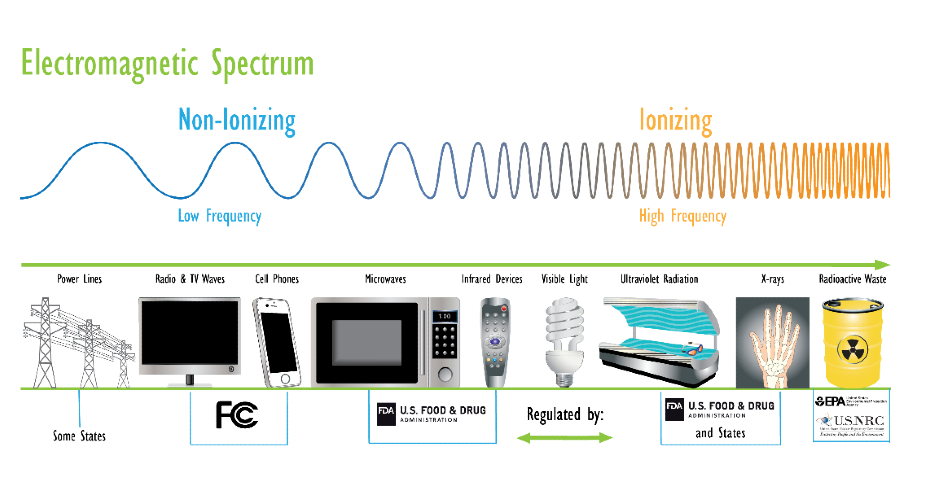
Every day, you and everyone around you are being bombarded with electromagnetic radiation. Now hold on, there’s no need to panic… unless you have digital electronic equipment and rely on telecommunication and transportation. The vast majority of this energy takes the form of non-ionizing radiation, which means that it doesn’t have nearly enough energy per quantum to ionize atoms or molecules. Figure 1 is a handy illustration of this.
However, when there are multiple sources of these electromagnetic “emissions”, it can cause havoc in our day-to-day lives by disrupting electronic equipment such as our phones, our computers, airplanes, satellites and even our cars. In the best of circumstances, these disruptions are merely benign glitches in normal operations, but as our society becomes more and more dependent on electronic equipment managing many aspects of our lives, the results of these disruptions could be catastrophic [1-5].
When powered, every piece of electronic equipment emits its own electromagnetic radiation; and the more equipment that is housed in one place, the more radiation it is generating [6]. Every piece of equipment functions at a specific low frequency wavelength, and if the signals are crossed then it can cause disruptions in their operation. This is referred to as electromagnetic interference, or EMI for short. One of the methods of preventing these signals from interfering with our equipment is to shield the electronic components from them. This is typically done by encasing the components in a metal mesh or highly specialised materials, such as rubber loaded with conductive carbon fibre fillers [7] or even polystyrene foam with conductive carbon nanotubes or graphene [8], tailored for the purpose of blocking out interference. These structures do come with their own drawbacks, however, such as: increased overall weight with the use of the metal mesh; degradation of the conductive rubber due to exposure to UV and handling; and fragility and brittleness of the polystyrene foam. The manufacturing methods for all of these also rely on the use of a mould, which is an added cost to the manufacturing process and means that changes to the geometry of the final product cannot be altered quickly.
One of the aims of TEAM-A is to use additive manufacturing (AM), also known as 3-D printing, to create materials that would provide shielding against EMI. There are many factors which determine EMI shielding, including the material type, thickness, and wavelength of the interference signals. EMI shielding refers to the reflection and/or absorption of EM radiation. The ability of a material to shield against interference is represented and explained by the shielding effectiveness formula (Figure 2)
Here P-in- and P-out- are the power of incident and transmitted waves through a shielding material; SE-A- and SE-R- are the shielding effectiveness values from absorption and reflection respectively; and SE-M- represents multiple reflections in the shielding. SE-A- and SE-R- are given by the following formulas (Figure 3).
Here στ is the total conductivity of the material, μr is the relative permeability of free space, εο is the permittivity of air, and w is angular frequency of the alternative current created by the wave of frequency f: 2Πƒ.
With absorption loss, the amplitude of an electromagnetic wave passing through an absorptive material decreases exponentially; this in turn causes heating of the material due to the induced currents in the material that cause ohmic losses. The absorption loss for this material increases with frequency, which means that these materials possess high conductivity and permeability, with a sufficient thickness that is required to shield against the lowest threat frequency (Figure 4).
There have been many instances of AM being used successfully in attempts to create materials that would provide shielding against interference [9-11]. However, one of the main challenges that researchers are still faced with when using AM technology is the ability to achieve axially-aligned filler particles and aspect ratios which will allow for multiscale controlled manufacturing. The ability to achieve filler alignment is a significant step in creating a material that can shield against EMI. If fibrous fillers are used, aligning them can give us multiple options: the ability to achieve complete shielding against interference signals, or - if alignment is carried out in specific directions and patterns - we can tailor electromagnetic properties of the printed materials such that they are anisotropic (i.e. angle-dependent), controlling and filtering different wavelengths and polarisations as required.
Some advancement has been made with filler alignment by using fused filament fabrication in which the alignment of fibrous fillers has been achieved by melting and forcing polymers loaded with randomly orientated fillers, either fibres or flakes, through a narrow nozzle [12]. But some may ask what does all this mean, and what are the benefits to using AM technology as opposed to more conventional, tried and tested methods of manufacturing?
One way that using AM could benefit EMI shielding capabilities is the ability to create parts in an expedited manner while reducing the final weight of the component and, depending on the type of AM used, cutting costs associated with design and manufacturing. Conventionally manufactured metal meshes and rubber loaded with conductive material can be up to three times heavier than an EMI shielding component manufactured using AM technology, although conventionally manufactured shielding using metal sheets and mesh is typically thinner than AM components. However, one of the biggest advantages of using AM for EMI shielding is the ability to create bespoke and intricate parts, with the added advantage of speedily modifying their geometry as needed before manufacture.
The goal of our project is to create a method of additive manufacturing, using selective laser sintering of polymer powders and conductive fillers, in order to produce novel materials that will provide:
- Tailored EMI/RF shielding properties
- Multiscale controlled manufacturing
- Shielding against acoustic vibrations and interference
- Axially aligned filler particles and aspect ratios which will allow for multiscale controlled manufacturing
- Multimaterial printing
- The ability to withstand high impacts, vacuum, and radiation.
There are several key findings that have been made in our project thus far. Current progress has led us to develop and test various prototypes to aid in the creation of axially aligning fillers and fabrication of graded structures by alternating the deposition of varying powder blends to create a composite material during the printing process. The purpose of the prototype is twofold: to provide alignment of fillers, and as a means of creating selective multi-material printing for the SLS process, something which is lacking for this method of additive manufacturing (AM). During these tests we investigated deposition patterns, the influence of the hopper geometry and nozzle size on powder flow and deposition, and the effect that deposition speed had on the uniformity of the deposited layer. The goal has been to achieve a 100 to 120µm layer thickness; this is of great significance, as a successful print using SLS technology requires thin layer deposition in order for the laser to effectively melt the powder.
This work involved creating a hopper style attachment which is intended for insertion into the laser sintering printer that operates in tandem with the standard deposition system of the powder bed systems. Using the hopper prototype we varied the materials used, combining PA12 with various fillers such as glass beads, chopped carbon fibre, PTFE powder and graphite flakes to determine the effects on deposition and filler alignment. We have made good progress with the development of the prototype and have entered into the second phase of testing, where we will be producing a metal prototype which will be loaded into a desktop SLS printer to test its performance using typical printing conditions.
The research that we are performing at the Centre for Additive Layer Manufacturing (CALM) at the University of Exeter can have a significant impact in the AM industry. The selective multi-material printing with the ability to align fibrous filler in situ during the printing process is a very attractive proposition for the fabrication of many products. This in itself has many added benefits, including the ability to create novel and bespoke components that can provide shielding against interference signals, which is of growing concern in the consumer market, as well as in more specialised areas such as medicine, aviation, military and defence.
[1] Boeing Commercial Airplane Group, Statistical Summary of Commercial Jet Aircraft Accidents: worldwide operations 1959-95, 1996.
[2] RTCA Portable Electronic Devices Carried on Board Aircraft, report of RTCA Special Committee 177, RTCA Report DO-233, 20 August 1996.
[3] Lucca, G., 2016. Electromagnetic interference from power lines on pipelines: influence of pipe insulating coating degradation. International Transactions on Electrical Energy Systems, 26(12), pp.2699-2712.
[4] Siergiejczyk, M., Pas, J. and Rosinski, A., 2016. Issue of reliability–exploitation evaluation of electronic transport systems used in the railway environment with consideration of electromagnetic interference. IET Intelligent Transport Systems, 10(9), pp.587-593.
[5] Carolyn Ritchie, Potential Liability from Electromagnetic Interference with Aircraft Systems Caused by Passengers' On-Board Use of Portable Electronic Devices, 61 J. Air L. & Com. 683 (1996)
[6] Bagotia, N., Choudhary, V. and Sharma, D., 2018. A review on the mechanical, electrical and EMI shielding properties of carbon nanotubes and graphene reinforced polycarbonate nanocomposites. Polymers for Advanced Technologies, 29(6), pp.1547-1567.
[7] Zhan, Y., Oliviero, M., Wang, J., Sorrentino, A., Buonocore, G., Sorrentino, L., Lavorgna, M., Xia, H. and Iannace, S., 2019. Enhancing the EMI shielding of natural rubber-based supercritical CO2 foams by exploiting their porous morphology and CNT segregated networks. Nanoscale, 11(3), pp.1011-1020.
[8] Yan, D., Ren, P., Pang, H., Fu, Q., Yang, M. and Li, Z., 2012. Efficient electromagnetic interference shielding of lightweight graphene/polystyrene composite. Journal of Materials Chemistry, 22(36), p.18772.
[9] Zakar, E., Anthony, T. and Dubey, M., 2019. Effects of conductive polymer composite layering on EMI shielding during additive manufacturing. MRS Advances, 4(38-39), pp.2153-2159.
[10] Vovrosh, J., Voulazeris, G., Petrov, P., Zou, J., Gaber, Y., Benn, L., Woolger, D., Attallah, M., Boyer, V., Bongs, K. and Holynski, M., 2018. Additive manufacturing of magnetic shielding and ultra-high vacuum flange for cold atom sensors. Scientific Reports, 8(1).
[11] Ecco, L., Dul, S., Schmitz, D., Barra, G., Soares, B., Fambri, L. and Pegoretti, A., 2018. Rapid Prototyping of Efficient Electromagnetic Interference Shielding Polymer Composites via Fused Deposition Modeling. Applied Sciences, 9(1), p.37.
[12] Brenken, Bastian & Barocio, Eduardo & Favaloro, Anthony & Kunc, Vlastimil & Pipes, Byron. (2018). Fused Filament Fabrication of Fiber-Reinforced Polymers: A Review. Additive Manufacturing. 21. 10.1016/j.addma.2018.01.002.
Figure References:
[i] Yong, Ching & Rahman, Tharek & Chew, Kim Mey. (2015). Wireless industry emission: Electromagnetic field monitoring and analysis. 10. 9800-9807. Yong, Ching & Rahman, Tharek & Chew, Kim Mey. (2015). Wireless industry emission: Electromagnetic field monitoring and analysis. 10. 9800-9807.
[ii] Saini, Parveen & Arora, M.. (2012). Microwave Absorption and EMI Shielding Behavior of Nanocomposites Based on Intrinsically Conducting Polymers, Graphene and Carbon Nanotubes. 10.5772/48779.
.jpg)
.jpg)
.jpg)